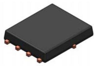
Welcome to BEAM! Tel: +86-553-5896615
Language: Help


Specification
| Product Attribute | Attribute Value |
| PPAP | No |
| SVHC | Yes |
| EU RoHS | Compliant with Exemption |
| Mounting | Surface Mount |
| ECCN (US) | EAR99 |
| Packaging | Tape and Reel |
| Pin Count | 8 |
| Automotive | No |
| Lead Shape | No Lead |
| PCB changed | 8 |
| Part Status | Obsolete |
| Channel Mode | Enhancement |
| Channel Type | N |
| Configuration | Dual |
| Package Width | 5.8 |
| Package Height | 1 |
| Package Length | 4.9 |
| Product Category | Power MOSFET |
| Supplier Package | PQFN EP |
| Maximum IDSS (uA) | 1@Q 1|500@Q 2 |
| Process Technology | TMOS |
| Standard Package Name | QFN |
| SVHC Exceeds Threshold | Yes |
| Typical Fall Time (ns) | 3@Q 1|5@Q 2 |
| Typical Rise Time (ns) | 3@Q 1|5@Q 2 |
| Number of Elements per Chip | 2 |
| Maximum Gate Resistance (Ohm) | 2@Q 2|3.2@Q 1 |
| Minimum Gate Resistance (Ohm) | 0.1 |
| Maximum Power Dissipation (mW) | 2200@Q 1|2500@Q 2 |
| Typical Gate Charge @ 10V (nC) | 21@Q 1|64@Q 2 |
| Typical Gate Charge @ Vgs (nC) | 21@10V|10@4.5V@Q 1|64@10V|30@4.5V@Q 2 |
| Maximum Gate Source Voltage (V) | ±20@Q 1|±12@Q 2 |
| Typical Output Capacitance (pF) | 1195@Q 2|397@Q 1 |
| Typical Turn-On Delay Time (ns) | 9@Q 1|12@Q 2 |
| Maximum Drain Source Voltage (V) | 30 |
| Typical Gate Plateau Voltage (V) | 2.4@Q 2|3.2@Q 1 |
| Typical Turn-Off Delay Time (ns) | 21@Q 1|38@Q 2 |
| Maximum Diode Forward Voltage (V) | 1.2 |
| Typical Diode Forward Voltage (V) | 0.77@Q 2|0.84@Q 1 |
| Typical Gate to Drain Charge (nC) | 2@Q 1|9@Q 2 |
| Maximum Gate Threshold Voltage (V) | 2.7@Q 1|2.5@Q 2 |
| Minimum Gate Threshold Voltage (V) | 1.2@Q 2|1.1@Q 1 |
| Typical Gate Threshold Voltage (V) | 1.5@Q 2|2@Q 1 |
| Typical Gate to Source Charge (nC) | 4.5@Q 1|9@Q 2 |
| Typical Reverse Recovery Time (ns) | 33@Q 2|25@Q 1 |
| Maximum Operating Temperature (°C) | 150 |
| Minimum Operating Temperature (°C) | -55 |
| Maximum Continuous Drain Current (A) | 13@Q 1|30@Q 2 |
| Operating Junction Temperature (°C) | -55 to 150 |
| Typical Input Capacitance @ Vds (pF) | 1485@15V@Q 1|4150@15V@Q 2 |
| Typical Reverse Recovery Charge (nC) | 41@Q 2|9@Q 1 |
| Maximum Drain Source Resistance (mOhm) | 8@10V@Q 1|1.8@10V@Q 2 |
| Maximum Gate Source Leakage Current (nA) | 100 |
| Maximum Positive Gate Source Voltage (V) | 12@Q 2|20@Q 1 |
| Maximum Pulsed Drain Current @ TC=25°C (A) | 140@Q 2|70@Q 1 |
| Maximum Power Dissipation on PCB @ TC=25°C (W) | 2.5@Q 2|2.2@Q 1 |
| Typical Reverse Transfer Capacitance @ Vds (pF) | 117@15V@Q 2|37@15V@Q 1 |
| Maximum Continuous Drain Current on PCB @ TC=25°C (A) | 30@Q 2|13@Q 1 |
| Maximum Junction Ambient Thermal Resistance on PCB (°C/W) | 120@Q 2|125@Q 1 |
| Description |
Related products
Inquiry Price
Popular Products
