Welcome to BEAM! Tel: +86-553-5896615
Language: Help


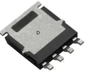
MOSFETs SQJ420EP-T1_GE3
Vishay
SQJ420EP-T1_GE3
--
Diodes, Transistors and Thyristors
MOSFETs
Specification
| Product Attribute | Attribute Value |
| Tab | Tab |
| PPAP | Yes |
| EU RoHS | Compliant |
| Mounting | Surface Mount |
| Packaging | Tape and Reel |
| Pin Count | 5 |
| Automotive | Yes |
| Lead Shape | Gull-wing |
| PCB changed | 4 |
| Part Status | Active |
| Channel Mode | Enhancement |
| Channel Type | N |
| Configuration | Single Triple Source |
| Package Width | 4.37 |
| Package Height | 1.07 |
| Package Length | 4.9 |
| Product Category | Power MOSFET |
| Supplier Package | PowerPAK SO |
| Number of Elements per Chip | 1 |
| Maximum Gate Resistance (Ohm) | 2.1 |
| Minimum Gate Resistance (Ohm) | 0.65 |
| Maximum Power Dissipation (mW) | 45000 |
| Typical Gate Charge @ 10V (nC) | 27 |
| Typical Gate Charge @ Vgs (nC) | 27@10V |
| Maximum Gate Source Voltage (V) | ±20 |
| Typical Output Capacitance (pF) | 193 |
| Maximum Drain Source Voltage (V) | 40 |
| Typical Gate Plateau Voltage (V) | 2.4 |
| Maximum Diode Forward Voltage (V) | 1.2 |
| Typical Diode Forward Voltage (V) | 0.79 |
| Maximum Gate Threshold Voltage (V) | 2.5 |
| Minimum Gate Threshold Voltage (V) | 1.5 |
| Typical Gate Threshold Voltage (V) | 2 |
| Typical Reverse Recovery Time (ns) | 28 |
| Maximum Operating Temperature (°C) | 175 |
| Minimum Operating Temperature (°C) | -55 |
| Maximum Continuous Drain Current (A) | 30 |
| Operating Junction Temperature (°C) | -55 to 175 |
| Typical Input Capacitance @ Vds (pF) | 1427@25V |
| Maximum Drain Source Resistance (mOhm) | 10@10V |
| Maximum Positive Gate Source Voltage (V) | 20 |
| Maximum Pulsed Drain Current @ TC=25°C (A) | 110 |
| Maximum Junction Ambient Thermal Resistance on PCB (°C/W) | 70 |
| Description |
Related products
Inquiry Price
Popular Products
