Welcome to BEAM! Tel: +86-553-5896615
Language: Help


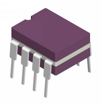
Op Amps TLC4502MJGB
Texas Instruments
TLC4502MJGB
--
Amplifier
Op Amps
Specification
| Product Attribute | Attribute Value |
| HTS | 8542.33.00.01 |
| PPAP | No |
| SVHC | Yes |
| Type | Low Offset Voltage Amplifier |
| EU RoHS | Not Compliant |
| Mounting | Through Hole |
| ECCN (US) | EAR99 |
| Packaging | Tube |
| Pin Count | 8 |
| Automotive | No |
| Lead Shape | Through Hole |
| Output Type | CMOS |
| PCB changed | 8 |
| Part Status | Active |
| Rail to Rail | Rail to Rail Output |
| Package Width | 7.11(Max) |
| Package Height | 5.08(Max) - 0.51(Min) |
| Package Length | 10.16(Max) |
| Supplier Package | CDIP |
| Manufacturer Type | Low Offset Voltage Amplifier |
| Minimum CMRR (dB) | 90 |
| Power Supply Type | Single|Dual |
| Shut Down Support | No |
| Process Technology | CMOS |
| Standard Package Name | DIP |
| SVHC Exceeds Threshold | Yes |
| Minimum CMRR Range (dB) | 90 to 95 |
| Typical Slew Rate (V/us) | 2.5@5V |
| Typical Voltage Gain (dB) | 120 |
| Supplier Temperature Grade | Military |
| Typical Settling Time (ns) | 2200 |
| Number of Channels per Chip | 2 |
| Typical Output Current (mA) | 100(Max) |
| Maximum Power Dissipation (mW) | 1050 |
| Maximum Quiescent Current (mA) | 3.5@5V |
| Maximum Dual Supply Voltage (V) | ±3 |
| Maximum Input Bias Current (uA) | 0.00006@±2.5V |
| Minimum Dual Supply Voltage (V) | ±2 |
| Typical Dual Supply Voltage (V) | ±3 |
| Maximum Input Offset Current (uA) | 0.00006@±2.5V |
| Maximum Input Offset Voltage (mV) | 0.1@±2.5V@-55C to 125C |
| Maximum Single Supply Voltage (V) | 6 |
| Minimum Single Supply Voltage (V) | 4 |
| Typical Single Supply Voltage (V) | 5 |
| Maximum Operating Temperature (°C) | 125 |
| Minimum Operating Temperature (°C) | -55 |
| Typical Gain Bandwidth Product (MHz) | 4.7 |
| Typical Input Noise Voltage Density (nV/rtHz) | 70@5V |
| Typical Noninverting Input Current Noise Density (pA/rtHz) | 0.0006@5V |
| Description |
Related products
Inquiry Price
Popular Products
